Electrical Vias
Vias are components that connect a metal layer with another one that is above or below it using via shapes.
Those shapes are also used in the electrical ports in the via.
It is possible to create your own via by using ElectricalVia.
GenericElectricalVia is a more generic class in which a list of different shapes and layers can be defined.
ElectricalVia
- class ipkiss3.pcell.via.cell.ElectricalVia
Class for common electrical vias. Its purpose is to electrically connect two layers (
layer_topandlayer_bottom) that are defined in the Layoutview. Two ports/terms namedtopandbottomrefer to the connection points on those respective layers. The connection is done with a connection layer(layer_via)- Parameters:
- name: String that contains only ISO/IEC 8859-1 (extended ASCII py3) or pure ASCII (py2) characters
The unique name of the pcell
Views
- class Layout
A standard electrical via is made of a boundary on three layers (
layer_top,layer_bottomandlayer_via). For each layer (top,bottomandvia) 2 properties are defined:top_shape
top_layer
analogous properties are defined for the other layers.
- Parameters:
- via_shape: Shape
viashape of the via.- via_layer: Layer
Drawing layer for the
vialayer of the via.- bottom_shape: Shape
Shape used for the
bottomof the via. Also used as shape in thebottomport.- bottom_layer: Layer
Drawing layer for the
bottomof the via.- top_shape: Shape
Shape used for the
topof the via. Also used as shape in thetopport.- top_layer: Layer
Drawing layer for the
topof the via.- view_name: String that contains only alphanumeric characters from the ASCII set or contains _$. ASCII set is extended on PY3.
The name of the view
- Other Parameters:
- layers: locked
- shapes: locked
Examples
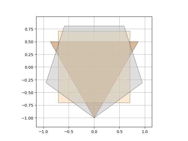
import si_fab.all as pdk  # noqa: F401
from ipkiss3 import all as i3
from ipkiss3.pcell.via.cell import ElectricalVia

cell = ElectricalVia()
# defining the shapes that are going to be used
# For the top bottom layer and via layer you can either define a layer or
# a combination of a process and a purpose.

layout = cell.Layout(
    top_shape=i3.ShapeRegularPolygon(n_o_sides=3),
    bottom_shape=i3.ShapeRegularPolygon(n_o_sides=9),
    via_shape=i3.ShapeRegularPolygon(n_o_sides=5),
    top_layer=i3.TECH.PPLAYER.M1.LINE,
    bottom_layer=i3.TECH.PPLAYER.M2.LINE,
    via_layer=i3.TECH.PPLAYER.V12.PILLAR,
)

layout.visualize()
GenericElectricalVia
- class ipkiss3.pcell.via.cell.GenericElectricalVia
Most generic class for electrical vias. Its purpose is to electrically connect two layers (
layer_topandlayer_bottom) that are defined in the Layoutview. Two ports/terms namedtopandbottomrefer to the connection points on those respective layers.- Parameters:
- name: String that contains only ISO/IEC 8859-1 (extended ASCII py3) or pure ASCII (py2) characters
The unique name of the pcell
Views
- class Layout
Layout view of a generic via. Adds all the shapes contained in the property
shapesonto layer defined in the propertylayers.By default those properties are determined with the help of other properties refering to two layers (
topandbottom) that are most commonly used in vias. For each layer (topandbottom) 2 properties are defined:top_shape
top_layer
analogous properties are defined for the bottom layer.
- Parameters:
- layers: list and List with type restriction, allowed types: <class ‘ipkiss.primitives.layer.Layer’>
List of layers used to make the via
- shapes: list and List with type restriction, allowed types: <class ‘ipkiss.geometry.shape.Shape’>
List of shapes used to make the via
- bottom_shape: Shape
Shape used for the
bottomof the via. Also used as shape in thebottomport.- bottom_layer: Layer
Drawing layer for the
bottomof the via.- top_shape: Shape
Shape used for the
topof the via. Also used as shape in thetopport.- top_layer: Layer
Drawing layer for the
topof the via.- view_name: String that contains only alphanumeric characters from the ASCII set or contains _$. ASCII set is extended on PY3.
The name of the view
Examples
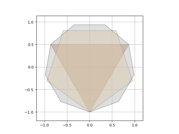
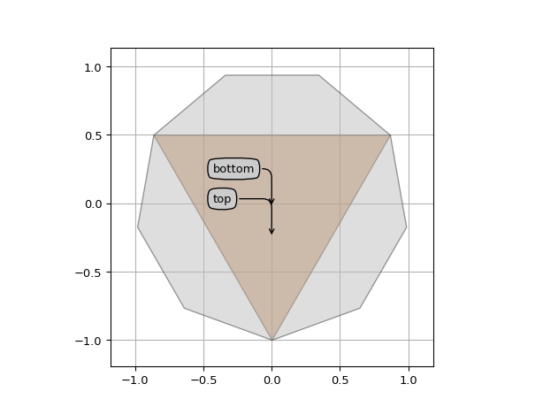
import si_fab.all as pdk  # noqa: F401
from ipkiss3 import all as i3
from ipkiss3.pcell.via.cell import GenericElectricalVia

cell = GenericElectricalVia()
# defining the shapes that are going to be used
# For the top and bottom layer you can either define a layer or a combination of and a purpose.

layout = cell.Layout(
    top_shape=i3.ShapeRegularPolygon(n_o_sides=3),
    bottom_shape=i3.ShapeRegularPolygon(n_o_sides=9),
    top_layer=i3.TECH.PPLAYER.M1.LINE,
    bottom_layer=i3.TECH.PPLAYER.M2.LINE,
)

layout.visualize(annotate=True)
import si_fab.all as pdk  # noqa: F401
from ipkiss3 import all as i3
from ipkiss3.pcell.via.cell import GenericElectricalVia

cell = GenericElectricalVia()
# defining the shapes that are going to be used
shapes = [i3.ShapeRegularPolygon(n_o_sides=i + 3) for i in range(3)]
# defining the corresponding layers that are going to be used
layers = [i3.TECH.PPLAYER.M1.LINE, i3.TECH.PPLAYER.V12.PILLAR, i3.TECH.PPLAYER.M2.LINE]
# If you set the shape array you have to explicitly set the properties relating to the
# top and bottom layers that are expected to be defined.
layout = cell.Layout(
    shapes=shapes,
    layers=layers,
    top_shape=shapes[0],
    bottom_shape=shapes[2],
    top_layer=layers[0],
    bottom_layer=layers[2],
)
layout.visualize()